
Application technology and advantages of gallium nitride in switching power supply
The use of gallium nitride (GaN) in power applications is an important innovation, and it is hopeful that it will make a significant contribution to achieving the goal of high-efficiency power conversion. GaN is a semiconductor material that has been put into use and is widely used in the field of LED lighting and the increasingly important wireless field. With the progress of technology and the increase of failure rate, GaN provides many advantages in applications such as AC and DC power conversion and level conversion.
Compared with previously used silicon (Si) transistors, GaN-based switching power transistors can operate at high voltages, with higher performance and lower losses.
GaN can work under high-frequency conditions and maintain high performance and high efficiency. The GaN device uses a GaN-on-Si process suitable for the existing Si manufacturing process. Because the volume of GaN devices is much smaller under the same current capability.
Therefore, compared with Si equivalent materials, GaN transistors are more cost-effective, which will make the application of GaN devices from large-scale industrial equipment to miniaturized handheld devices attractive. High-performance power supply design not only requires a higher operating frequency, and at the same time to achieve precise switching characteristics, and the huge advantages of GaN is driving the advent of the era of high-efficiency power conversion.
Today, power supply designers begin to rethink their circuit design, looking for ways to fully utilize the potential of the new GaN transistor power system, while avoiding the influence of harmful factors.
Traditional solutions usually start from the components themselves, such as GaN switches, Si switch drivers, high-speed switch controllers, power inductors, transformers, and capacitors; integrated circuit (IC) manufacturers that develop power products can provide collaborative systems Level solution, to achieve a substantial performance design improvement for customers, and even integrate multiple chips into a modular package.
GaN's position in the power supply chain
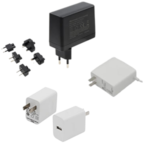
Most electronic equipment uses switching power supply (SMPS), which can effectively convert alternating current to direct current (AC to DC) and step voltage 110-120V, 220-240V or 12-, 5-, 3.3-V and other system needs Power supply range
These functions are very typical for consumer electronics and data centers. SMPS is also used in DC to DC conversion and renewable energy inverters, automotive electronics, industrial equipment and other types of high-power systems.
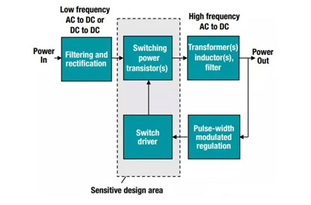
Figure 1 shows a block diagram of a typical SMPS workflow. SMPS rectifies the input voltage (usually high-voltage and low-frequency alternating current) into direct current. The power line filter is used to prevent high-frequency components generated in the power source from being reflected back during transmission. The high-frequency power switch (the core of SMPS) converts the direct current. The signal is converted into a pulse voltage waveform, and the output is regulated and filtered at the level required by the low-voltage system.
The feedback controller from the output is used to provide a pulse width modulation (PWM) signal to the power switch driver to realize the adjustment function; as the load demand changes, the signal pulse width will gradually increase or decrease.
Traditionally, power switches have used silicon MOSFETs (Metal Oxide Semiconductor Field Effect Transistors), but they are now being replaced by GaN FETs.
According to system design requirements, a variety of topologies can be used, from singleFET boost converters to multiple dual FET designs in the layout of power switches, up to 4 FET full-bridge converters.
Switches and their drivers are very sensitive parts of the entire design, because they must accurately complete each operation in accordance with the instructions of the controller, otherwise the work of the power supply system will become unstable.
In addition, due to the rapid rise and fall of the modulation voltage, noise is injected into the feedback loop, which will also cause instability of the power supply system. One requirement of all grid-connected systems is to isolate the part from the grid and the part provided for use by the power system, so as to ensure the safe use of user equipment.
Another problem is that the high-frequency operation during the power conversion process cannot be allowed to interfere with the transmission of power grid energy and generate unnecessary noise on the power transmission line.
GaN devices solve this isolation requirement through conversion operations at higher frequencies, effectively reducing the impact of electromagnetic interference; conversion at higher frequencies can reduce the size of isolation transformers and input filters.
Advantages of applying GaN in SMPS systems
In the application of power switches, GaN has more important advantages than silicon materials, because GaN can provide lower losses at higher voltages and use less energy during switching. After years of development, Si switches have been greatly improved, but under the same size and voltage conditions, GaN's excellent performance is unmatched by Si devices.
At present, Si MOSFET has a certain cost advantage compared with GaN, but as time goes by, the cost difference will become smaller and smaller.
The operating voltage range of GaN switching devices is very wide, so power supply designers can achieve higher switching frequencies within a wide range of input and output voltages, while achieving the desired design efficiency in a smaller physical size. The most valuable application of GaN is in power solutions that are as small as possible.
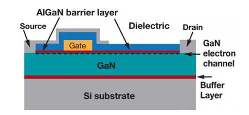
Figure 2 shows the basic structure of a GaN transistor. From the previous discussion, we can know that the GaN material is located on the Si substrate. The advantage of this design is that it can not only make full use of the advantages of decades of Si processing, but also take advantage of the advantages of the new material GaN. One of the advantages is that it can achieve higher Band gap voltage.
Semiconductors are a special type of material because the band gap energy is the voltage jump required to change this type of material from an insulator to a conductor. The band gap energy of 3.2 electron volts (eV) provided by GaN is almost three times that of Si.The
oretically, higher band gap energy means better performance at higher temperatures, because more heat can be maintained before the substance becomes a conductor; this inherent performance is expected to improve automobiles, Device performance in industrial and other high-temperature environments.
GaN development curve in SMPS design
Although GaN has many advantages, this technology is just beginning to enter the field of power supply design. Previous applications in the LED and wireless fields may give people an impression that the application of GaN in power supply design has already had better conditions.
In fact, the use of GaN in power FETs requires significant process and device development, making the development of such products slow. The difference between the new FET and Si devices makes IC suppliers and system designers exercise caution in the development phase, and gradually solve various complex problems encountered in the design.
Traditional GaN devices are usually in an on state or in a depletion mode, while silicon MOSFETs are enhanced devices that are turned off. In order to provide a direct replacement for silicon MOSFETs, GaN FET switch suppliers have redesigned their products to work in enhanced mode, or use a series switch to provide a normally-off function.
Replacing Si MOSFETs with GaN FETs is only the beginning of the redesign. The high frequency capabilities of GaN transistors require higher timing accuracy for switch drive signals. In addition, switches are highly sensitive to parasitic impedances from packages, interconnects, and external sources.
The integrated Si-based GaN driver can turn on and off the GaN switch at high speed, helping to promote the design of GaN switching power supplies. Mature silicon technology makes it possible to develop these extremely accurate, high-frequency adjustable drivers.
For example, TI’s LM5113 gate driver is designed to control mid-to-high-level high-end and low-end enhancement mode GaN power switches. The gate driver integrates the required components to achieve performance optimization. This integration can not only reduce the number of circuit boards. Space can also help simplify the design.
In addition to achieving high-precision drive timing with minimal delay, the device also provides important protection for the efficient and precise operation of the GaN switch. For example, the bootstrap clamp keeps the gate-source voltage in a safe operating area; high current pull-down can improve dv/dt immunity and prevent accidental low-side activation; independent source and drain pins can be optimized Turn on and turn off time to improve efficiency and reduce noise; and fast propagation delay matching can optimize the dead time during switching.
GaN-based SMPS system-level solution design
Combined with fast and accurate power management control, GaN gate drivers have a fairly advanced GaN-based SMPS design. Therefore, the optimization of the gate driver itself limits the improvement of SMPS performance, and even the shortest possible trace between the driver and the GaN switch will cause the delay time to vary with the design.
Future IC solutions will need to control the variability issues caused by the layout and design of passive devices, because these are critical to the coupling characteristics of the driver and the switch. Since the two devices discussed above are based on different materials and have very different characteristics, the cost of integrating them on a chip may still be relatively high in the near future.
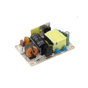
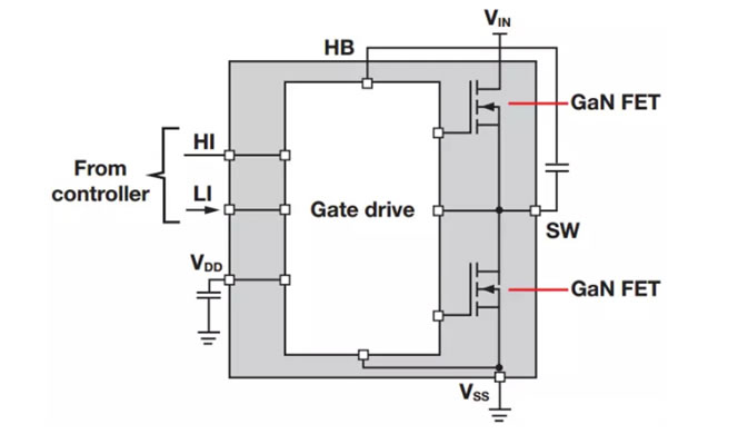
However, a single package module that integrates FETs, drivers, and passive devices that support switching (as shown in Figure 3) will greatly reduce the area and number of components of the SMPS; this size reduction also means a reduction in system manufacturing costs and GaN Improved design efficiency.
As important as the size reduction solution is to reduce the complexity of the design, the driver switch module will reduce the length of the connection between the chips, minimize the delay time and parasitic impedance, thereby reducing the distortion of the switching output pulse waveform. A well-designed module can greatly reduce the parasitic factors of multi-chip design, and may even drop by an order of magnitude or more.
Another important factor in providing system-level solutions is the controller-regulator, which must operate at the high frequency supported by GaN and must respond to changes in output voltage in real time. The time resolution must also meet the precise pulse width requirements to minimize conduction losses during the dead time.
Fortunately, digital power controllers can support these requirements and provide additional performance and I/O capabilities. TI provides comprehensive expertise in digital power control, combined with the company's power technology to provide system-level solutions for GaN regulation and control switches.
In addition, it is necessary to study magnetic components based on GaN design, because these components are still customized for silicon enabling frequencies. TI has cooperated with power supply manufacturers and GaN research institutes to continuously propose new design requirements to magnetic component suppliers according to the specific needs of the market.
As the use of GaN power devices continues to expand, magnetic device suppliers will be market-oriented and improve existing technologies. Once the time is right, the industry will be able to feel the benefits of GaN devices in many power applications.
GaN innovation will meet the needs of the future market
The continuous growth of the world's population and the acceleration of social development have made the demand for electricity continue to increase, and increasingly urgent environmental pressures force us to accomplish more things with less energy. When we try to address these needs, world development will benefit from innovations that help us provide, convert, and consume electricity more efficiently, resulting in technologies that improve our lives.
GaN is such an innovation, through which it is expected to reduce the power loss in power conversion, thereby helping us to obtain more benefits from limited energy. In order to meet the challenge of GaN, TI is making full use of its leading position in research and development to create solutions that can reduce the complex problems caused by high-frequency power conversion. These differentiated solutions will help simplify the design, save space and reduce the number of components, while minimizing signal delay and spurious interference.
With the emergence of these superior products, SMPS developers will be able to launch higher-performance systems at a faster speed. The success of high-performance systems will further promote GaN to enter new application areas, including high-power industrial equipment and low-power consumer goods markets. The modules and other key parts of the system-level solution will help us realize the full potential of GaN technology in terms of power efficiency.