


How to design GAN MOS drive circuit
Basic principles
2.1 Driving principle
GaN System's GS66502B gallium nitride transistor is a 650V/7A enhancement mode power device with a gate-source voltage range of −10 V to +7 V. Compared with the −4 V~6 V of the EPC series of GaN transistors, it has a wider input range. GS66502B has almost no switching loss and reverse freewheeling diode loss. Although there is no diode in the body, it has the characteristics of a diode [3]. That is, the reverse conduction of GaN enhancement mode transistors has an equivalent "diode" characteristic, which is related to the gate voltage. No need for external anti-parallel diodes, excellent reverse recovery performance, and high hard-switching efficiency.
In response to the requirement that the gate voltage of GaN transistors needs to be strictly controlled, TI has developed a dedicated GaN gate drive chip LM5114, which can strictly control the drive voltage, and the output voltage range can be adjusted between 4 V and 12 V. LM5114 can drive a single enhanced GaN transistor, with independent sink output function [4]. The independent pull-sink output function can control the turn-on and turn-off time separately by changing the drive resistance on each channel, which can avoid the adverse effect on the turn-off channel when the same drive resistance is used.
Figure 1 is a commonly used driving circuit for Si MOSFET devices. The commonly used driving circuit generally uses only one VO output pin. When the driving signal is high, the anti-parallel diode D1 is turned off, and the VCC of the driver charges the junction capacitance of the switch tube through the driving resistor RGON. When the driving signal is low, the anti-parallel diode D1 is turned on, and the conduction voltage drop generated by the anti-parallel diode is added between the gate and source. Because the threshold voltage of GaN power devices is very low, the threshold voltage of GS66502B is only 1.5 V. If the drive circuit that uses the source and sink shared output will cause the gate-source voltage to exceed the threshold voltage, the transistor will fail to turn off. In order to achieve the same drive function as the shared output pin circuit, and to avoid the use of diodes, a drive circuit that turns on and off the independent output can be used, as shown in Figure 2.
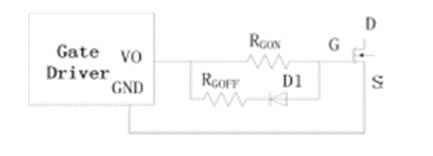
Figure 1. Driving circuit for common output of pullirrigation
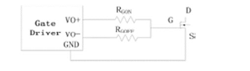
Figure 2. Driving circuit for independent pull irrigationoutput
2.2 Drive circuit design
The turn-on resistance controls the switching rate of turn-on, but too large turn-on resistance will reduce the switching rate and increase the loss. Too small turn-on resistance will increase the switching speed and increase the switching loss. This is due to the possible gate produced by Miller. oscillation. The commonly used turn-on resistance range of turn-off resistance is 1~2 Ω, which can provide powerful and fast gate drive pull-down for GaN transistors. For reverse dv/dt and reverse Miller current, a low impedance path is required to reduce the reverse gate spike voltage and the subsequent ringing caused by LC resonance. Therefore, by selecting the appropriate gate resistance, the speed of the GaN transistor can be well controlled by the gate resistance. The key is to choose the right RG(ON) and RG(OFF) to help stabilize the drive performance. In this paper, LM5114 is selected as the driver chip of GS66502B GaN device, and the basic driver circuit is designed, with an on-resistance of 5.1 Ω and an off-resistance of 1.8 Ω, as shown in Figure 3.
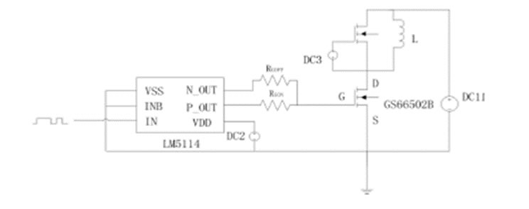
Figure 3. Double pulse test circuit using LM5114
2.3 Auxiliary power supply design
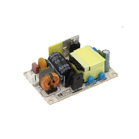
Since the driving voltage of GaN power devices is different from that of ordinary Si MOSFETs, the power supply voltage of the LM5114 used is also different, so in converter applications, an auxiliary power supply needs to be provided to power the drive chip. For GS66502B, the gate-source voltage range is −10 V~+7 V, and the optimal value for turn-on is 6 V, so an additional 6 V supply voltage is required. This article designs a 220 V to 6 V auxiliary power supply circuit based on LNK306PN, which can provide 6 V auxiliary power supply to GS66502B, as shown in Figure 4.
2.4 Double pulse principle
The principle of the double pulse test is that the drive circuit sends out two pulses, one wide and one narrow, and the GaN transistor is turned on and off twice. At t1, the wide pulse arrives, VGS rises, and the GaN transistor drops to the on-state voltage. The voltage across the DC power supply of the main circuit is almost all applied to the inductor, and the inductor current rises linearly. At this time, the conduction of the GaN transistor The current ID is equal to the inductor current IL. At t2, the wide pulse ends, VGS drops to zero, and the transistor is turned off at the same time it starts commutation with the equivalent diode, and the inductor current remains almost unchanged. At t3, the narrow pulse arrives, and the current in the circuit has reached a certain value, so it can effectively test the ability of the GaN transistor to turn on with load, and observe its commutation with the equivalent diode
Case. From t3 to t4, the current ID and IL continue to rise linearly until the energy stored in the inductor is completely consumed after the second turn-off.
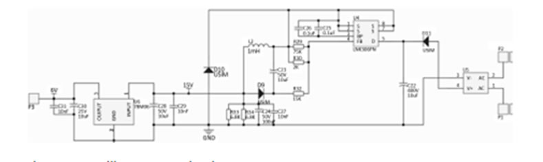
Figure 4. Auxiliary power circuit
With the development of technology, more and more GAN MOS drive circuits appear. Many manufacturers directly use an integrated IC to make the GAN drive circuit for everyone's design convenience. This not only facilitates everyone's design, but also provides a guarantee for the consistency and reliability of the subsequent mass-produced drive circuit. It can also maximize the advantages of GAN MOS.